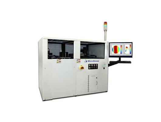


MicroSense new UltraMap C200 measurement system provides full wafer, high speed measurement of semiconductor material using fast accurate non contact capacitive sensors.
MicroSense capacitance sensor technology
provides full high resolution mapping on sawn, lapped, single side polished, or double side polished wafers in the production environment.
UltraMap C200 systems are available in both a low cost bench top system as well as a fully automated sorting configuration with up to six cassettes.
Complete Coverage:
• Thickness
• TTV/TIR/LTV/LTIR
• Bow/Warp
Fast, Accurate Measurements
• Throughput up to 90 wafers/hour 150mm
• >100,000 measured points
• 0.05μm TTV Repeatability
• 2D & 3D mapping capability
Production Friendly
• Sawn, Lapped and Polished wafers
• Non clean room environment
• Automated calibration
| Measurement Parameters | Accuracy | Repeatability One Sigma | Display Resolution |
| Thickness: Center, Minimum, Maximum, Average | ± 0.10 μm | 0.05 μm | 10 nm |
| Global Flatness: TTV TIR FPD | ± 0.05 μm | 0.05 μm | 10 nm |
| Local Flatness: Local Thickness Variation (LTV) Local Total Indicator Reading (LTIR) Local Focal Plane Deviation (LFPD) | ± 0.05 μm | 0.05 μm | 10 nm |
| Bow and Warp Bow Warp Sori | 0.5 μm + 0.5% of reading | 10 nm |
Wafer Specifications | System Configuration |
Diameters: 50mm, 100mm, 150mm, 200mm Diameter Tolerance: ± 0.5mm Thickness Range: 300 to 1400um Dynamic Range: Thickness: ± 50um Bow/Warp: ± 250um Surfaces: Sawn, Lapped, Polished Fiducials: Semi Flat, Notch | Wafer Handling: Robotic Measurement Positioning: Precision Air Bearing Pre-aligner: Optional OCR Reader: Optional SECS/GEM: Optional Cassette Stations: Up to 6 Calibration: Automated Reliability (MTBF): 10,000 |