


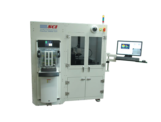
The FilmTek™ 2000M TSV advanced semiconductor packaging metrology system provides an unmatched combination of speed, accuracy, and precision for high-throughput measurements of resist thickness, through silicon vias (TSVs), Cu-pillars, bumps, redistribution layer (RDL) and other packaging processes.TSV etch depth and depth uniformity is critical to ensure high yield during TSV fabrication. The FilmTek™ 2000M TSV can readily determine etch depth for via structures with diameters greater than 1 µm up to a maximum etch depth of 500 µm. Additional capabilities include measurement of height or depth, critical dimension, and film thickness for microbumps, trenches, and a variety of other structures and applications.
Measurement function: TSV etch depth, bump height, critical dimension, and film thickness
Wafer handling: Brooks or SCI
Substrate size: 200 or 300mm
Pattern recognition: Cognex
CD precision (1σ): <0.2%
Etch depth precision (1σ): <0.005%
Film thickness range:
Film thickness precision (1σ): <0.005%
Light source: Halogen lamp
Detector type: 2048 pixel linear CCD array


