


Precision Wafer Thickness Measurement
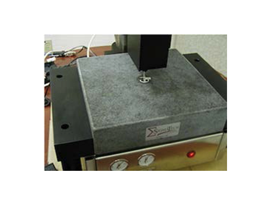
MicroSense’s UltraMap UMM-BP2 manual wafer dimesnional measurement system utilizes MicroSense proprietary auto-positioning backpressure probe technology to accurately measure thickness, TTV, bow and warp of wafers of any material up to 200 mm in diameter (350mm with extended base). The system provides an accurate measurement regardless of wafer surface finish, resistivity or optical characteristics.
This version of the system is designed to measure rigid wafers and substrates, and uses a two sided, dual probe measurement technique which is compliant with SEMI standards. The system includes a fixed lower probe and an auto-positioning upper probe. This provides very versatile measurement capability, since the system can measure wafers ranging from 100μm to 20mm thick without mechanical adjustment of the upper probe position. The system accommodates wafers with maximum warp or bow of 100 microns. Alternate systems are available for highly warped wafers, or thin flexible wafers.
By combining manual wafer positioning with an automated measurement, the system achieves lowest-possible cost while maintaining high accuracy and flexibility.
0.5μm absolute accuracy
Available verification standards
Available reference standards for high-thickness samples
Wide measurement range - 100μm to 20mm thickness
Warp range 100μm
Production Friendly
Sawn, Lapped and Polished wafers
Non clean room environment
Easy data export
Measurement Technology
The UltraMap-BP systems use exclusive patented backpressure sensing probes for precise measurement of all materials, whether conductive or non-conductive. The advantages of this sensing probe technology include:
Auto-calibration of backpressure sensors (no need for master wafers)
No need to adjust for different materials
Automatic adjustment to material thickness over a 2000μm range
| Measurement Parameters | Accuracy | Repeatability One Sigma | Display Resolution |
| Thickness: Flat Wafers (<100um Bow) Thickness: Center, Minimum, Maximum, Average | 0.5 μm | ± 0.015 μm | 0.1um |
| Wafer Specifications | System Configuration |
| Wafer Size: Any, including, and Custom and Saw-frame mounted. Wafer Thickness Range: 100μm - 3000μm Surfaces: Wafers - As Sawn, Lapped, Polished | Wafer Handling: Manual Wafer Measurement Location Positioning: Manual Calibration: Automated Wafer Measurement: Automated Reliability (MTBF): 50,000 Samples |
| Facilities Requirements |
| Dimensions: 18” width, 16” depth, 20” height. Separate PC, Monitor, Keyboard, and Mouse Weight: 100lbs Voltage: 110V for US, 200 – 250V options available. Single phase grounded polarized outlet required. Frequency: 50/60 Hz Current: 2A nominal, 10A peak Circuit Breaker: 10A UL489A certified breaker Air supply: Clean dry air or Nitrogen 40 – 60 PSI Fittings: ¼” compression fitting |