


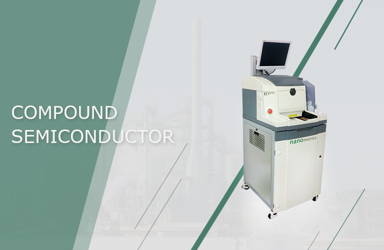

Semi- automated wafer metrology system for 50mm to 300mm wafers
Dual White Light Chromatic probes + single IR Interferometry probe
WLC interferometry probe for » air gap » measurement. (optional)
HISCAN mode for line or area scanning (optional)
Pattern vision & alignment module (Cognex)(optional)
Exclusive open, X-Y stage on air bearing with 10um positioning accuracy.
WLC Thickness measurement range : 20um to 3mm
IR Thickness measurement range : 20um to 1mm (in Si)
WLC Interferometry thickness measurement range : 1um to 200um (air gap)
Bow and warp measurement range up to 2500um.
Multiple wafer holding fixtures available : Open frame chuck with vacuum and dual-size 3-point open fixture.
SECS/GEM communication software (optional)
Overall class of equipment : Class 100
European rules and CE compliant
SEMI standards compliant.
User friendly operator interface
3 access security levels
Storage of 1000 settings and recipes
High reliability and dependability : Uptime over 95%.
It uses the principle of chromatic coding (variation of the refractive index as a function of wavelength) to measure the Z coordinate of each point of the surface on the sample.
The optical sensor includes an optical probe connected to a White LED (Lifetime over 10,000hours) through a fiber optic cable. This optical probe is mounted at the end of a shaft , which position is automatically adjusted to measure a wide thickness range as well as large bows.
The advantages of this sensing probe technology are numerous:
Auto-calibration of sensors.
Fast measurement (up to 4pts/sec)
Measurement independent of target material
Automatic adjustment to material thickness
Measurement of conductive and non-conductive material.
Measurement through transparent material (glass or tape)
Roughness measurement after backgrinding
0.5um accuracy
0.1um resolution
Wafer 4" to 12" (100 to 300mm) round or square
Thickness range: 20um to 1mm
Flexible recipe generation
2D & 3D mapping capability
SECS/GEM communication
For any flat wafer: Bow and warp < 250um
Thickness measurement: with WL technology
Accuracy: 0.5 mm (micron)
Repetitive accuracy: +/-0.15 micron)
Resolution: 0.05 micron
Linearity: 0.01%
Thickness measurement: With IR Interferometry:
Accuracy: 0.5um ± 0.1% of reading
Resolution: 0.05um
Acquisition frequency: up to 4 kHz
Linearity: Dependent on knowledge of RI
Bow and Warpage measurement:
Standard range: +/-2500mm
Accuracy: 3um + 0.5% of range.
| Wafer Specifications | System Configuration |
| Wafer Size: Any, including, and Custom and Saw-frame mounted. Wafer Thickness Range: 100μm - 3000μm Surfaces: Wafers - As Sawn, Lapped, Polished | Wafer Handling: Manual Wafer Measurement Location Positioning: Manual Calibration: Automated Wafer Measurement: Automated Reliability (MTBF): 50,000 Samples |
| Facilities Requirements |
| Dimensions: 18” width, 16” depth, 20” height. Separate PC, Monitor, Keyboard, and Mouse Weight: 100lbs Voltage: 110V for US, 200 – 250V options available. Single phase grounded polarized outlet required. Frequency: 50/60 Hz Current: 2A nominal, 10A peak Circuit Breaker: 10A UL489A certified breaker Air supply: Clean dry air or Nitrogen 40 – 60 PSI Fittings: ¼” compression fitting |


